UV or photo Nano Imprint Lithography (UV-NIL or P-NIL) is a versatile technique for low-cost nanoscale device fabrication. The precise, direct patterning and repeatable replication of complex three-dimensional nanoscale patterns (submicron, 10’s of nanometers) in a single step make the NIL technique compelling in comparison to other expensive techniques such as e-beam or helium ion beam lithography.
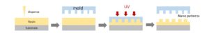
In the NIL method, a resin is coated on a substrate, a stamper with patterns is pressed on, and the resin is cured by UV light as illustrated. ACW has a full line of UV resins for use in UV-NIL from replications of nano features on glass wafer or plastic substrate to replications of nano features for waveguides.
Go to the Nano-Imprint Lithography application page for product listings. Click HERE to open the high RI LuxNIL® product brochure. ACW recently teamed up with EV Group to demonstrate high resolution (50 nm), high RI (up to 1.96 at 633 nm) UV-NIL with sub-nm height gain per imprint on 25 imprints on a single working stamp; see the Whitepaper HERE.
In addition to nano imprint resins, ACW offers a full line of optically clear, high RI, solvent free resins for micro imprint applications for wafer level optics and micro lens arrays. ACW’s micro imprint resins offers refractive index of 1.51 to 1.6. Click HERE to open the P-NIL brochure with product descriptions.