Photo Nano-Imprint Lithography (P-NIL)

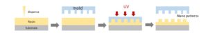
UV or photo nano-imprint lithography (UV-NIL or P-NIL) is a versatile method for low-cost nano-scale device fabrication. A resin is coated on a substrate, a stamper with patterns is pressed on, and the resin is cured by UV light as illustrated below. The method gives embossed features on plastic, glass, silicon, or metal for many applications including optical storage, diffractive optical elements (DOE), displays, semi-conductor devices. ACW provides low viscosity, high hardness, high Tg, and optically clear resins for accurate nano-scale replications. And ACWs stable of P-NIL resins now includes very high RI (1.70 to 1.96 at 589 nm) LuxNIL® resins for AR/VR/MR applications.
| ACW | Featured P-NIL Products | Data |
| P-NIL resins | Multi-purpose for spin coat process | |
| BD-119 | Nano/micro structures, RI589nm = 1.5165, Tg 131 °C | TDS |
| BD-218 | Nano/micro structures, RI589nm = 1.506, Tg 120 °C | TDS |
| BD-400 | Nano/micro structures, RI589nm = 1.510, Tg 145 °C | TDS |
| IP-158 | Nano/micro structures, RI589nm = 1.584, Tg 70 °C | TDS |
| IP-159B | Nano/micro structures, RI589nm = 1.589, Tg 75 °C | TDS |
| PR-1600-CA | Nano/micro structures, RI589nm = 1.600, Tg 89 °C | TDS |
| PR-1612 | Nano/micro structures, RI589nm = 1.612, Tg 60 °C | TDS |
| PR-1614 | Nano/micro structures, RI589nm = 1.614, Tg 76 °C | TDS |
| Lens resins | wafer-optics lenses, micro-lens arrays | |
| L2002-C42 | Microlens arrays, hybrid lens, RI589nm = 1.515, Tg 150 °C, η = 2,800 cps | TDS |
| L2002-C56 | Microlens arrays, hybrid lens, RI589nm = 1.513, Tg 145 °C, η = 1,200 cps | TDS |
| L2007 | Microlens arrays, hybrid lens, RI589nm = 1.567, Tg 109 °C | TDS |
| L2061-B | Microlens arrays, hybrid lens, RI589nm = 1.602, Tg 130 °C | TDS |
| Very High RI resins | Augmented and Virtual Reality, Diffractive Optical Elements, LuxNIL® | |
| P270-U | RI589nm = 1.71 | TDS |
| P276-U | RI589nm = 1.80 | TDS |
| P283-U | RI589nm = 1.83 | TDS |
| P285-U | RI589nm = 1.91 | TDS |
| P288-U | RI589nm = 1.94 | TDS |
| P289-U | RI589nm = 1.96 | TDS |
PDF brochure for high RI Resins for Microimprint
Do you need a custom designed resin?