Photo Nanoimprint Lithography (P-NIL) promises to be a rapid and low cost methodology for manufacturing optical, electronic and optoelectronic micro-scale and nano-scale devices. One obstacle for the methodology is the high cost of molds or masters that will have a finite lifetime in terms of multiple copies. The work-around for this cost is to use a master mold to produce working stamps that can then be used for many copies of the imprinted devices. Working stamps can be hard with a rigid glass backplane or soft with a flexible polymeric backplane such as treated PET.
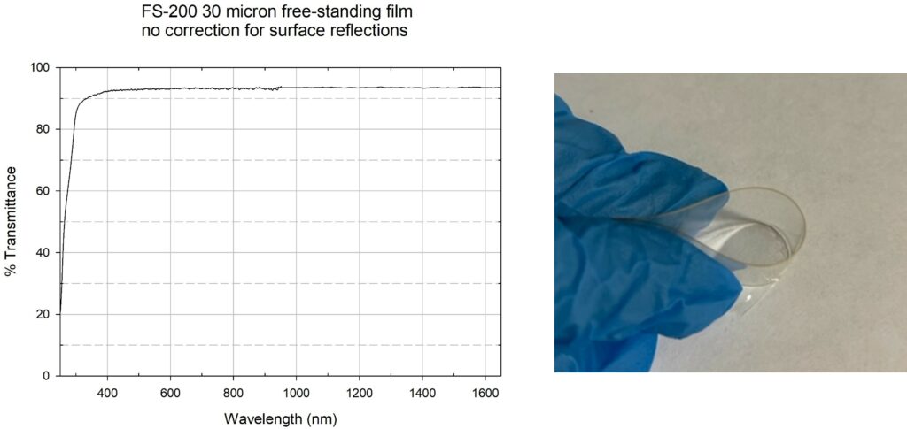
ACW has now released photo-cure resins for both hard and soft working stamps. These resins cure with 2,000 mJ/cm2 of LED 365 nm light which is delivered in a few seconds with conventional UV-curing equipment. The resins have moderate viscosity for use in spin coating or dispense coating. The cured hard stamp resin has a Tg and an elastic modulus similar to those of polycarbonate. The cured soft stamp resins have similar high Tgs and elastic moduli (both much greater than those of polydimethylsilicone, PDMS) while maintaining very high flexibility as shown below.
Click HERE for a brochure describing ACW’s Stamp Resins. Contact us at info@addisoncw.com to inquire about samples.